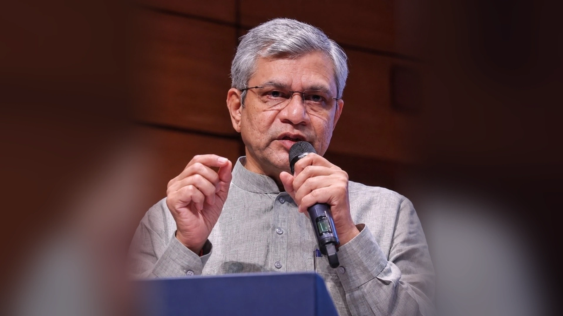
India must urgently develop and manufacture its own machinery and high-precision components required for semiconductor production, Union Minister for Electronics and Information Technology Ashwini Vaishnaw announced. Speaking on the expansion of the domestic silicon roadmap, the minister emphasized that building indigenous semiconductor equipment is essential for India to establish a truly self-reliant and sovereign chipmaking ecosystem.
Key Highlights of the Semiconductor Machinery Initiative:
- Indigenous Tooling Mandate: Union Minister Ashwini Vaishnaw calls for localized manufacturing of semiconductor fabrication tools, robotic handling units, and high-precision equipment.
- Strategic Value Chain Expansion: Broadens the national semiconductor blueprint beyond wafer fabrication and packaging (ATMP/OSAT) into upstream capital goods and precision engineering.
- Geopolitical Insulation: Aims to reduce dependency on foreign equipment monopolies and safeguard domestic fabrication facilities against global export curbs and supply chokepoints.
- Upcoming Policy Support: Government aligning incentives under India Semiconductor Mission 2.0 to support precision component suppliers, specialized metallurgy, and cleanroom hardware.
India Semiconductor Equipment Manufacturing: Strategic Pillars and Ecosystem Targets
| National Policy Directive | Indigenous Semiconductor Machinery and Tooling Manufacturing |
| Announcing Authority | Ashwini Vaishnaw, Union Minister for Electronics and IT, MeitY |
| Primary Strategic Objective | Domestic manufacturing of semiconductor fabrication and packaging machinery |
| Critical Hardware Sub-Sectors | Precision optics, vacuum chambers, toxic gas delivery lines, cleanroom robotics |
| Targeted Production Facilities | Commercial wafer fabs, ATMP/OSAT assembly plants, compound semiconductor units |
| Upstream Supply Dependencies | Overcoming foreign monopolies across US, European, and Japanese equipment makers |
| Supporting Policy Framework | India Semiconductor Mission (ISM) and planned ISM 2.0 capital incentives |
| Ecosystem Stakeholders | Domestic capital goods manufacturers, IIT research consortia, global tooling partners |
Global Tooling Monopolies and India’s Domestic Machinery Roadmap
Semiconductor manufacturing equipment represents the single most complex and capital-intensive link in the global electronics supply chain. Currently, specialized lithography, etching, and chemical vapor deposition machinery are tightly controlled by a handful of international manufacturers. As demonstrated during the recent global tech shifts and leadership changes analyzed in our NVIDIA semiconductor supply chain report, concentrated equipment monopolies leave emerging production hubs vulnerable to international export restrictions and prolonged delivery cycles.
To counter this exposure, the Ministry of Electronics and Information Technology is formulating targeted support to incubate domestic precision engineering firms. Rather than attempting to replicate advanced extreme ultraviolet lithography immediately, India’s initial phase will target high-precision mechanical fixtures, ultra-pure fluid handling systems, and advanced testing sub-assemblies. This hardware push mirrors the sovereign technological self-reliance seen in the recent India indigenous AI models launch, ensuring that domestic wafer plants operating in Gujarat and Assam develop durable, localized equipment supply lines.
PFD Context
Minister Vaishnaw’s announcement marks an essential transition from semiconductor consumer to industrial builder. Subsidizing wafer fabrication lines without domestic tooling creates a fragile ecosystem entirely reliant on imported spare parts and proprietary foreign software locks. By fostering high-precision engineering and equipment component manufacturing at home, India can embed itself permanently into global semiconductor supply chains while securing true technological sovereignty.